74LCX125 Description
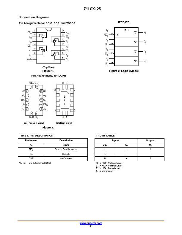
The LCX125 contains four independent non−inverting buffers with 3−STATE outputs. The inputs tolerate Voltages up to 5.5 V Allowing the interface of 5 V Systems to 3 V Systems. The 74LCX125 is fabricated with an advanced CMOS technology to achieve high Speed operation while Maintaining CMOS Low Power Dissipation.
74LCX125 Key Features
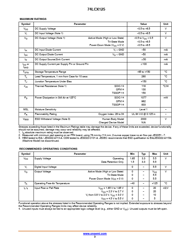
- 5 V Tolerant Inputs and Outputs
- 1.65 V-5.5 V VCC Specifications Provided
- 6.0 ns tPD max. (VCC = 3.3 V), 10 mA ICC max
- Power Down High Impedance Inputs and Outputs
- Supports Live Insertion/Withdrawal
- 24 mA Output Drive (VCC = 3.0 V)
- Latch-up Performance Exceeds JEDEC 78 Conditions
- ESD Performance
- Pb-Free DQFN Package
- These are Pb-Free Devices